Persistence: Shuji Nakamura and the Blue Light LED
Success comes from persistence.
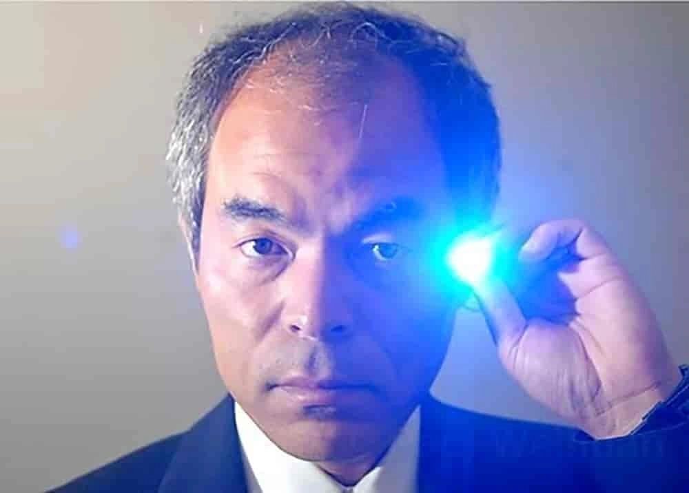 Shuji Nakamura
Success comes from persistence.
Persistence is the quality that allows someone to continue doing something, even though it is difficult or opposed by other people.
Why is persistence important for success?
Firstly, natural talent will only take you so far. What’s needed is a stead fast determination or persistence to keep at it, even when times are tough.
Aesop’s fable of the tortoise and the hare, clearly illustrates persistence.
Despite being naturally outclassed by the hare in a race involving speed, the persistence of the tortoise allows it to beat the hare and succeed.
Secondly, challenges are inevitable on your journey to success. Persistence means that you don’t give up when things get hard and you are able to push through to achieve success.
Everyone knows the inventor of the light bulb, Thomas Edison. But do you know who developed the first viable blue light LED prototype that led to the white light LED that is used in most lighting applications today?
The man is Shuji Nakamura, and his work on developing the blue light LED is a case study in persistence. LEDs have been around for a long time, but the blue light LED was the breakthrough that allowed LED technology to progress to make LEDs affordable and practical for everyday lighting use.
Before Nakamura developed the blue light LED, many people believe it to be impossible to create. To put things into perspective, and to show you how difficult, I’m going to tell you about the history and the science behind LEDs.
The science of LEDs
LEDs or Light Emitting Diodes, are semiconductors that emit light when a current flows through it.
A semiconductor is a material that has electrical conductivity that falls between a conductor such as copper and an insulator, such as glass. The most common semiconducting materials are crystals. Depending on the material of which the crystal is made, the conducting properties can be altered in useful ways, including light emission.
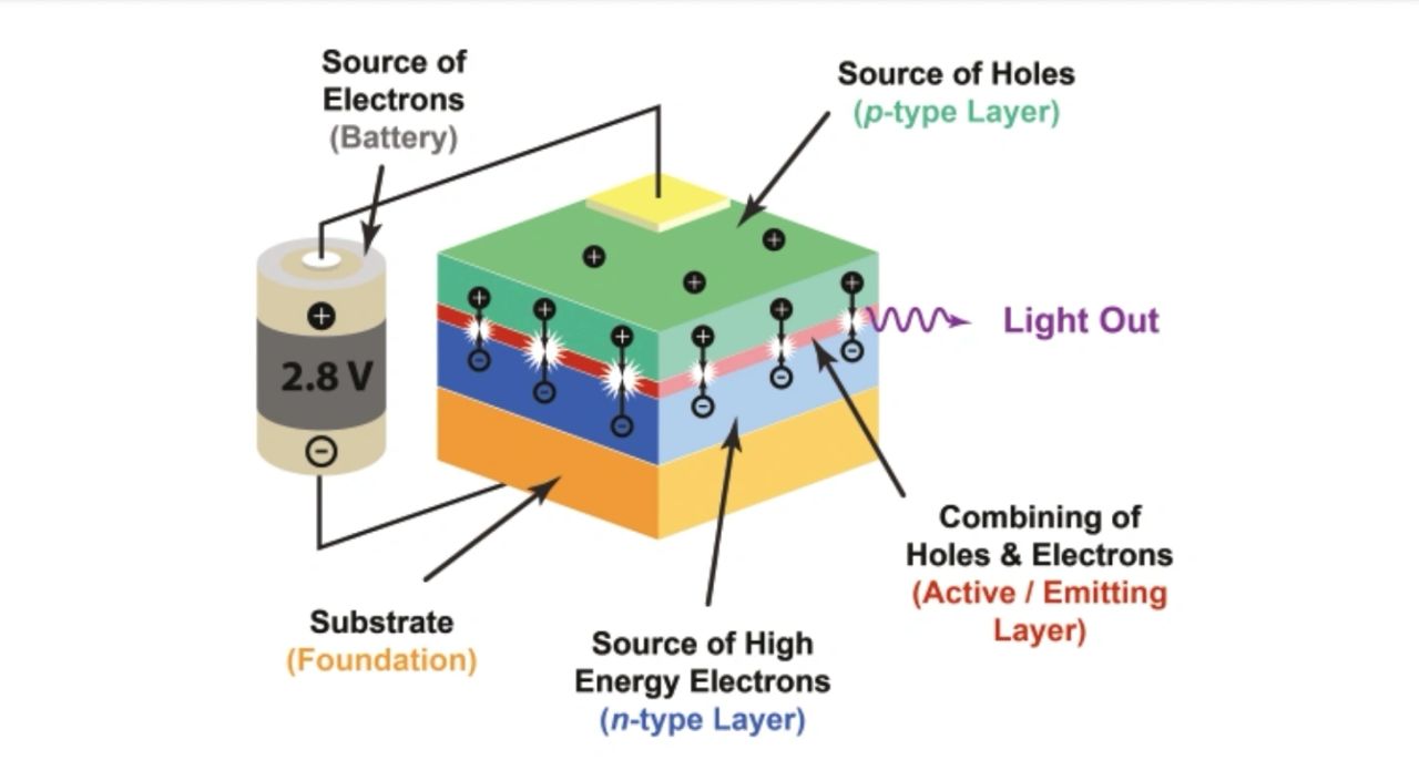
Light is produced in LEDs when current is passed through and the electrons move from the n-type material to the p-type material. N-type material has an excess of electrons, and p-type material has missing electrons or “holes”, and when electricity is applied, the electrons jump from the n-type region to the p-type region to fill the holes. The space between these two regions is called the energy band gap. When the electrons move, they release energy in the form of photons or light.
The size of the gap determines the amount of energy required for the electron to make the jump. The energy of the photon determines the type of light released, whether it is infra-red light (low energy) to ultraviolet (higher energy). Visible light sits in between infra-red and ultra-violet light on light spectrum and the colour of the visible light is determined by the specific levels energy. All this happens at the atomic level, hence the challenge for those trying to create the right materials for the right frequency to get the right colour of light.
The history of LEDs
Electroluminescence was discover in 1907. This is where a material emits light in response to the passage of an electric current.
The first LED was invented in 1927, but it was of no practical use due to its inefficiency in producing visible light.
It wasn’t for another 35 years until the first visible light LED was created in 1962. It emitting a red coloured light, but this was very dim and was costly to make.
Further research and development by various corporations increased the light output and reduced production costs, and in 1968, the red light LEDs became practical and commercially viable for consumer applications as instrument indicators and calculator displays.
The green LED was created in the 1970s, and when combined with red, was able to produce yellow light.
Further developments in the 1980s led to increase in the brightness which made possible the availability of ultra-bright orange-red, orange, green and yellow LEDs.
Despite over 50 years of LED development, it was still not possible to use LEDs for lighting as LEDs did not produce white light.
Blue light was needed to be combined with red and green to produce white light.
Although blue light LED was initially discovered in 1972, it did not produce the brightness needed for lighting applications due to the technical challenges.
At the time, many considered creating blue light LEDs too difficult, due to the inability to make the materials, and this was true for twenty years.
Shuji Nakamura and the blue light LED
But then, in 1993, a researcher named Shuji Nakamura made the necessary breakthroughs to produce a blue light LED bright enough to be used for lighting.
His is a story of persistence in the face of immense challenges. The industry had tried and didn’t believe it was possible. The company he worked for didn’t believe it was possible. His peers didn’t believe it was possible.
Nakamura worked as an engineer at an industrial electronics business called Nichia. Nichia started in 1956 and by 1966, through significant research and development, came up with innovations in phosphor manufacture which lead it to being a producer and supplier of phosphors for colour television.
Nichia was producing LEDs in the 1980s, but was suffering from over a decade of losses in a crowded and competitive market.
In 1988, Nakamura pitched the idea of developing the blue light LEDs to the company founder and president, Nobuo Ogawa. Nobuo Ogawa was an innovator and supported Nakamura, approving funding for him to begin his quest for the blue light LED.
To create a blue light LED, Nakamura needed to overcome three barriers:
- The manufacture of a high quality crystal, the material need for the blue light LED.
- The creation of the p-type of that crystal, in order for the LED to function.
- And for the LED to have sufficient light power output to be practical.
Between 1988 and 1993 Nakamura achieved the three breakthroughs that led to the creation of the first practical blue light LED.
- High quality crystal. The crystal used for LEDs were manufactured in labs. Crystals needed to have minimal defects at an atomic level, as defects disrupted the electron flow, which resulted in heat radiation instead of light. At the time, no one could produce the crystal of sufficient quality needed for blue light LEDs. After gaining the support of Nobuo Ogawa, Nakamura travelled from Japan to the United States to the University of Florida as a visiting research associate to learn how to use a new crystal manufacturing method called Metal Organic Chemical Vapor Deposition or MOCVD. An MOCVD reactor is essentially a giant oven that could mass produce clean crystal by passing a gas of molecules over a heated wafer. This creates the ultra-thin, single crystal layers needed for semiconductor use.
Working in the lab, Nakamura faced many challenges. Firstly he wasn’t allowed to use the working MOCVD, so he had to spend the first 10 months assembling a new system from scratch. Secondly, the researchers looked down upon him as they all had their PhDs and Nakamura did not. They treated him like a lowly technician and this experience created a strong desire in Nakamura to obtain his PhD.
After 12 months, he returned to Japan with an intimate knowledge of how an MOCVD reactor worked, a $2million MOCVD reactor for Nichia and a the dream to get a PhD. In Japan, at the time, it was possible obtain a PhD degree by publishing 5 scientific papers. This was called a paper degrees and he did not need to go to university to get this degree
There were two options of crystal for blue light LEDs, Zinc Selenide and Gallium Nitride. Both were semiconductors with theoretical band gaps in the blue light range however Zinc Selenide was the more promising option, as when grown, had less than 1,000 defects per square centimetre. Gallium Nitride had been abandoned by almost everyone because it was more difficult to create and had over 10 billion defects per square centimetre.
Nakamura decided to pursue Gallium Nitride as he was confident that he could publish many papers on this and earn his PhD. Nakamura reasoned that low interest in Gallium Nitride meant less competition and this meant that he had a greater chance of his research papers being accepted for publication. Interestingly, he had no confidence that he could actually invent the blue light LED, his objective was to get a PhD.
For six months, Nakamura tried to grow a Gallium Nitride crystal using his new MOCVD reactor without success. The reactor was designed for Gallium Arsenide and was not able to produce Gallium Nitride. Given the substantial investment in the reactor, he realised this was a big problem, so he decided to modify the reactor so it could produce the Gallium Nitride crystal. His 10 months of building an MOVDC reactor from scratch suddenly proved to be invaluable. Nakamura’s daily routine was to arrive at the lab at 7am and to modify the reactor until 1pm. Then in the afternoon, he would perform a couple of growths and analyse the results until 7pm. He would then go home and return the next day at 7am to repeat the process. He did this every single day, including weekends for 18 months, only taking time off on New Year’s Day.
Management had changed at Nichia, and Nakamura was ordered to stop researching the blue light LED due to costs. But having invested so much time and personal effort, Nakamura ignored these demands by Nichia management and continued to experiment.
In 1990, whilst going through this process, he invented a new MOCVD design that he called the two-flow MOCVD. Using this, he was able to create a very uniform and high quality Gallium Nitride crystal that had electron mobility that was 4 times higher than any other grown in a lab. He now had the highest quality Gallium Nitride crystal ever made.
- P-type Gallium Nitride. The second barrier to overcome was to create p-type Gallium Nitride. Scientists could create n-type Gallium Nitride, but p-type has been elusive for 20 years. A method to create p-type existed, this involved exposing individual crystals to a low-energy electron beam, which was not scalable. In addition to this, why this actually created p-type Gallium Nitride was not known. In 1992, Nakamura discovered that hydrogen was the reason why p-type Gallium Nitride was so difficult to produce. For MOCVD growth of Gallium Nitride, ammonia is used as the nitrogen source. Ammonia is made up of nitrogen and hydrogen atoms. The process introduced the hydrogen atom to the crystal, filling up the space that would allow it to act as an acceptor, therefore preventing it from being a p-type with a hole to accept electrons. Nakamura believed that energy was needed to release the hydrogen, so instead of used the electron beam, Nakamura used a process called annealing which heated the Gallium Nitride crystal to 400 degrees celsius. This caused the hydrogen to diffuse out of the crystal, enabling it to act as an acceptor and therefore create p-type Gallium Nitride. The added advantage of the thermal annealing method was that it was quick and could be used on any size crystal. This was better than the electron beam method and made it suitable to the mass production p-type Gallium Nitride.
With a reliable and simple method of making p-type crystal, Nakamura had all the materials necessary to create a prototype blue light LED.
In 1992, he presented the prototype blue light LED at an industry workshop and received a standing ovation. But despite his prototype being the best to date, it was still a blue-violet colour and extremely inefficient, with a light output power of 42 microwatt, well below the 1,000 microwatt threshold needed for practical use.
- Increase power by x100. This was the final hurdle to overcome. The solution was to increase the efficiency of electrons and the way to do this was to introduce an active layer which encouraged more electrons to jump from the n-type to p-type crystal.
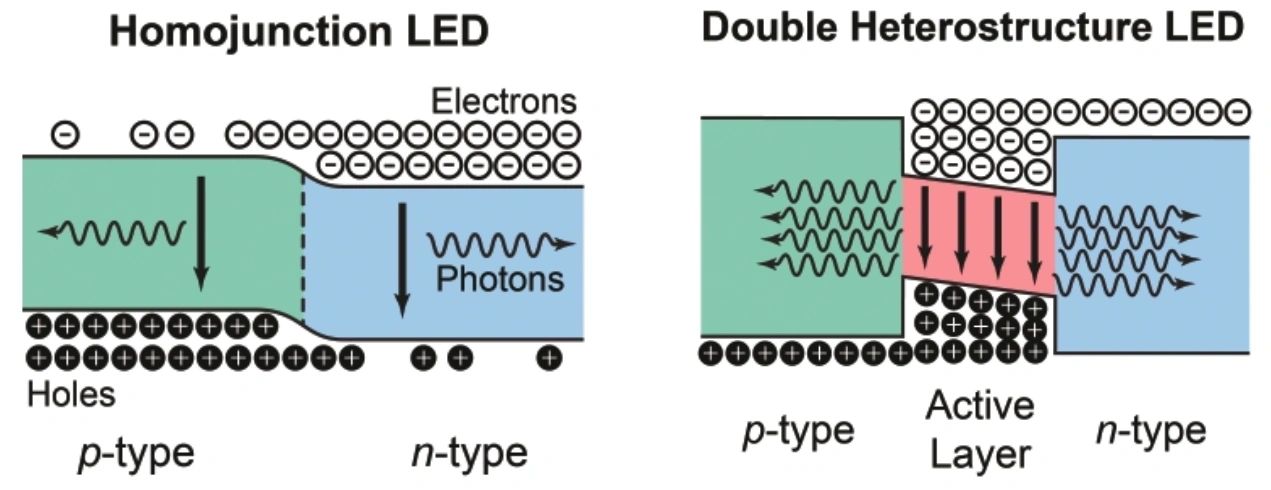
This design, with an active layer, called a double heterostructure LED, existed, but the challenge was again the material. The best material for the active layer was known to be Indium Gallium Nitride, as it shrunk the band gap to produce the active layer and also allowed for the tuning of the colour of the light by adjusting the amount of indium in the crystal. Creating Indium Gallium Nitride was more difficult than creating p-type crystal. Indium has high vapour pressure, so the typical growth temperature of Gallium Nitride meant Indium would boil off the surface and not incorporate into the crystal. Growing a lower temperatures resulted in poor crystal quality, along with defects and impurity. To achieve this, the MOCVD reactor requires precise control over all growth parameter and superior uniformity across the entire surface to achieve the desired result. Because Nakamura was able to modify his MOCDV reactor, he was able to force Indium onto the Gallium Nitride in precisely controlled production process to create Indium Gallium Nitride. Once this was achieved, the electrons flowed well, a little too well, and he needed to spend another couple of months to achieve the correct balance. He solved this problem with another crystal, Aluminium Gallium Nitride, this had a larger band gap and effectively trapped the electrons to cross exactly where it was needed. These improvements meant that Nakamura was able to create the first commercially available blue light LED that produced 1,500 microwatts of light power in 1994
Because of the blue light LED, Nakamura went on to create the white light LED, and then blue laser diode which is used for blu-ray discs and HD DVD.
Conclusion
Nakamura was recognised with many awards and in 2014 received the Nobel Prize for Physics, for the invention of efficient light-emitting diodes, which has enable bright and energy saving white light sources.
Persistence is one of the most important ingredients of success. Shuji Nakamura, the inventor of the blue light LED displayed this throughout his career. He overcame social, technical and corporate challenges to achieve what many believed to be impossible to achieve. His persistence helped to change the way we live in this world.
Image credits:
https://www.nobelprize.org/uploads/2018/06/nakamura-lecture.pdf
References:
https://www.youtube.com/watch?v=AF8d72mA41M
https://en.wikipedia.org/wiki/Light-emitting_diode#Single-color_LEDs
https://www.shineretrofits.com/lighting-center/lighting-resources/history-of-led-lighting/
https://en.wikipedia.org/wiki/Shuji_Nakamura
https://en.wikipedia.org/wiki/Light-emitting_diode
https://electronics.howstuffworks.com/led.htm
https://www.nobelprize.org/uploads/2018/06/nakamura-lecture.pdf